Building on the success of the Advanced CMOS workshop series in 2019-20 and AMS training in March 2020, CMC provides this training in partnership with Cadence Design Systems and GlobalFoundries®.
This is an advanced course that trains students in the Analog-Mixed Signal Design Methodology using Cadence tools targeting the GF12LP FinFET PDK. Course participants will have an opportunity to fabricate a chip targeting the GF12LP PDK facilitated by CMC. This can be a stand-alone learning opportunity or combined with a design fabrication opportunity. The training material has been developed by Cadence.
Important Notes:
- This course is not for beginners and requires familiarity with Cadence tools and prior chip fabrication experience. Please ensure you can check all the boxes in the section Pre-requisites prior to paying for your registration.
- Because course participants will have access to other proprietary and confidential information during the course, each participant is required to sign an Access to Intellectual Property & Non-Disclosure Agreement (NDA). This NDA will be emailed to eligible individuals that meet the pre-requisites.
Training Schedule
| Date | Time | Location |
|---|---|---|
| May 10 to 21, 2021 | 12:30 p.m. to 5:30 pm EDT | Online-Virtual session |
| Even Dates (May 10, 12, 14, 18, 20) | 12:30 p.m. to 3:00 p.m. EDT | Lecture, Demo and Lab start. |
| 3:00 p.m. to 3:30 p.m. EDT | Break | |
| 3:30 p.m. to 5:30 p.m. EDT | Self-paced Lab work | |
| Odd Dates (May 11, 13, 17, 19, 21) | 1:00 p.m. to 3:00 p.m. EDT | Office Hours: Cadence Engineers will be available to answer your questions related to the Labs |
Technology Description
- 3D FinFET transistor technology on 12nm CMOS technology
- Standard cells and IP libraries are from IP vendors (Users to arrange access. Not through CMC)
- GF12LP Features:
- Logic Voltages → Vnom: 0.8 V, Vmax: 0.945 V
- 4 VTs: SLVT / LVT / RVT / HVT
- IO offering: 1.2 V, 1.35 V, 1.5 V and 1.8 V EG Devices
- Well resistor, precision MOL resistor, MIM / MIM4 / APMOM / MOS / VNCAP capacitors, ESD, eFuse, VPNP, VNPN and Diodes, Inductors, Transmission line
- Interlevel Low-K and Ultralow-K dielectrics
- Packaging options: C4 solder, Round or Oblong Copper Pillar Bump, Micro pillar Bump
- Fabrication is carried out at a GF FAB in USA.
Reference Design, Design Flow, and Labs
The Reference Design is developed using the GF12 FinFET process and will include both analog and digital blocks.
The Reference Design will be adequate to demonstrate the following disciplines:
- Schematic preparation
- Layout and placement preparation
- Layout routing
- Layout finishing
- Digital design flow for mixed-signal
The Reference Flow Documentation has been developed as a collection of lectures, each demonstrating a separate portion of the development. The documentation will be delivered in PDF format and soft copies will be provided to the students and marked confidential information. Hard copies will not be provided.
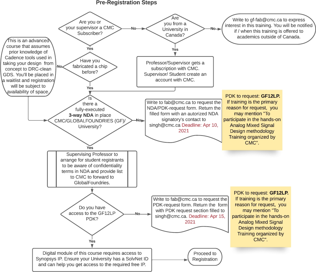
Pre-requisites
All students must be able to check all the following boxes to complete the prerequisites before their registration request is processed for the course (Limit: 30 attendees)
- I/my supervisor has a subscription with CMC and I have an account with CMC.
- I have taped out at least one design prior to this course
- Please check this box if your fabrication experience was with CMC
- My University has a fully executed 3-way NDA in place with CMC and GlobalFoundries
- I/my supervisor/university has a GlobalFoundryView (GFV) account and access to the GF12LP PDK for purposes of this training.
- If you have checked the first two boxes but do not have the NDA or PDK access in place, please contact fab@cmc.ca and ask for the NDA/PDK access request form to start the process.
- Complete the following self-paced learning and recommended reading:
- Cadence AMS methodology training based on gPDK45, access can be obtained by emailing licensing@cmc.ca
- View the webinar How Row-Based Methodology Improves Custom Layout
- Other material will be posted and needs to be reviewed before registration.
Registration
Registration is open to CMC subscribers who have completed the following pre-registration steps.
The price for registration is $500 for a CMC subscriber.
The class is full and the registration is closed.