Packaging

Low-temperature Co-Fired Ceramic (LTCC) Fab at ÉTS 

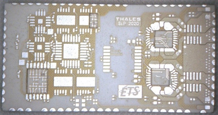
Overview  LTCC technology is a general-purpose multi-layer ceramic process used in various areas, namely:   Medical sensors and electronics  Automotive electronics   Satellite electronics and other vehicles in harsh environments  RF/microwave/mm-wave communications  CMC provides access to LTCC prototyping and other related services through the LTCC@ÉTS laboratory. Technical support on the LTCC process and access to the design […]

Low-temperature Co-Fired Ceramic (LTCC) Fab at ÉTS  Read More »

Generic Aluminum Nitride Carriers for Optoelectronic Applications

Overview These carriers are designed primarily for DC characterization. However, the layouts include 50-ohm co-planar GSG bias lines with 500-micron pitch. The laser carrier includes provision for inclusion of wire bonds to power up to six independent sections and accommodates a device with up to a 3 mm cavity length. The waveguide device is shorter,

Generic Aluminum Nitride Carriers for Optoelectronic Applications Read More »

Close up of laser cleaving

Laser-Assisted Cleaving

Overview The estimated turnaround time for this service is four to six weeks. Processing takes place at INO. Laser is used to trigger the location of cleaving. The cleaving is done with an accuracy of +/-15 µm. The technique provides good facet quality for end-fire coupling. Thin Silicon layers are accepted (up to 5 µm). For chip dimensions, see Guidelines

Laser-Assisted Cleaving Read More »

Flip-Chip Assembly Services

For MEMS and microelectronic device applications requiring a small footprint and short interconnects, our flip-chip assembly service offers access to die bumping or die-to-die/die-on-board flip-chip bonding. Whether your chip was fabricated through CMC services, a university-based fabrication facility, or elsewhere, we can help by providing competitive pricing, access to quick-start documentation, and engineering support.

Flip-Chip Assembly Services Read More »

Scroll to Top
Skip to content