Overview
- The estimated turnaround time for this service is four to six weeks.
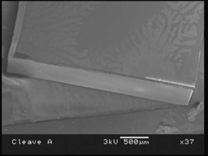
- Processing takes place at INO.
- Laser is used to trigger the location of cleaving.
- The cleaving is done with an accuracy of +/-15 µm.
- The technique provides good facet quality for end-fire coupling.
- Thin Silicon layers are accepted (up to 5 µm).
- For chip dimensions, see Guidelines for Laser Assisted Cleaving.
- We recommend alignment marks on chips to indicate where the cleaving is needed.
Applications
- Intended for use with Silicon photonics and other Silicon-based chips
- Cleaving along vertical plane of the waveguide
- Singulation of specific area of a chip