The smart technology revolution has enabled a myriad of complex functions to be integrated into increasingly tiny, sophisticated physical devices.
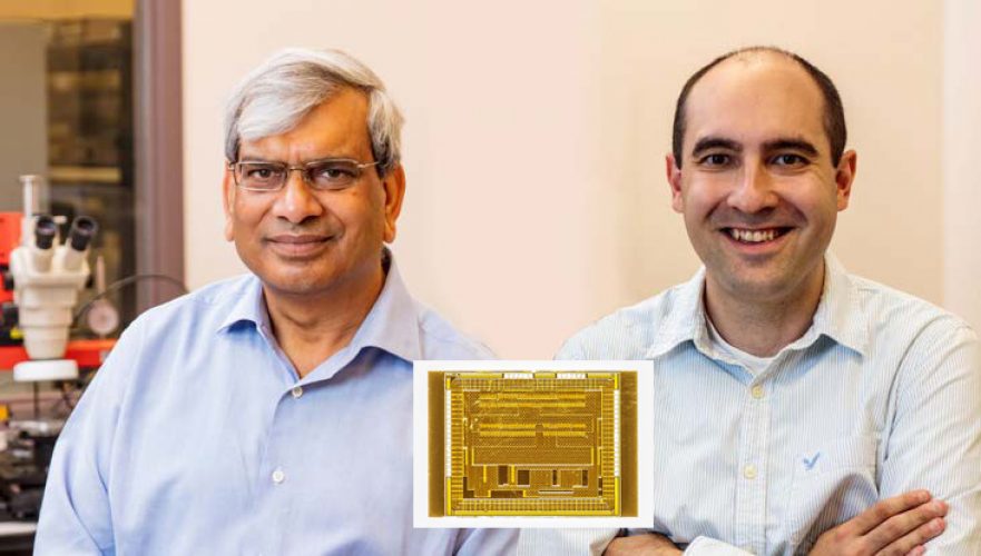
But the technologies that power these devices haven’t adapted so well to miniaturization. Now one of Canada’s leading experts in power electronics and his graduate student have developed a new power solution in a tiny chip with significantly higher power efficiency.
“Unfortunately, while devices have gotten smaller, their power technologies haven’t,” says Praveen Jain, Director of the Centre for Energy and Power Electronics Research (ePOWER) at Queen’s University. “The chips that power these devices need a lot of discrete components such as capacitors and transformers. It makes it difficult to make a monolithic power converter on a tiny chip.”
As Tier 1 Canada Research Chair in Power Electronics and the founder of two startup companies, Professor Jain has built his career on finding better solutions for harvesting, transmitting and consuming power in more cost-effective, energy-efficient ways. For example, Jain and his team have developed and advanced several generations of energy- and cost-efficient solar microinverters for residential use. Home systems need microinverters to convert direct current generated by the panels into alternating current compatible with the power grid.
Now his lab has produced a technology that shows potential to make that power conversion function even more efficient.
Our goal was to develop a device that could efficiently process the energy produced by power sources,” says Marko Krstic, a PhD candidate in Dr. Jain’s lab. “We wanted this circuit to be efficient and miniature and focused on creating a structure that would be well-suited for monolithic integration on a single chip.”
The key was to dispense with magnetic elements, traditionally used to convert and transfer energy, he says. “On-chip, integrated magnetic components, at this stage, have not developed to the point where we can use them effectively for power applications so we used capacitors exclusively in our design, which are more suitable for integrated implementations.”
Their technology, called a switched-capacitor converter, addresses a significant shortcoming of existing switched-capacitor devices, which typically operate at lower efficiencies than traditional magnetics-based converters. “This means that a significant amount of the energy processed by these devices is wasted as heat,” Krstic says.
“We looked at the performance limits of these structures and tried to determine exactly how efficient they could be at a fundamental level, which is something that wasn’t entirely clear in the past.”
Based on a comprehensive analysis of these structures involving network theory, Krstic optimized his converter to improve its power processing capability. The project took about five years and resulted in a chip with efficiency up to 20 percent higher than existing commercial chips.
This was a significant accomplishment, Jain says. “Previously there was no systematic approach to do this – it was just a black art. He developed the approach that enabled manufacturability.”
“There are limitless numbers of topologies and it’s not always clear which are the best for each application,” Krstic says. “Through our analysis, we could determine an optimal converter structure for any set of operating conditions.”
‘Previously there was no systematic approach to do this – it was just a black art. He developed the approach that enabled manufacturability’.
Their patent-pending converter has many applications, including mobile devices and electronics, but the real potential is in solar energy, where it could be integrated into the solar cells inside the PV panel.
“It’s particularly well suited for this application because we can apply it at the cell level to extract the maximum power from each solar cell,” says Krstic. “This is possible with our converter because it’s miniature, efficient, and silicon-based.”
None of this work would have been possible without CMC’s help, the researchers say. “If CMC wasn’t there, we’d never have built that chip,” says Jain. “They played a critical role in terms of advancing this particular technology. They not only provided the tools, they also helped us fabricate the whole thing.”
“This was the first integrated circuit I designed and I was fortunate enough to be able to consult with some of the knowledgeable engineers at CMC,” Krstic says. “The subsidized pricing helped us tremendously as well from a cost standpoint. Working with CMC has been a great experience. I feel I’m in a better position to contribute and to continue working on cutting-edge research.”
“It was extremely important to me to be able to implement my design,” he adds. “You can do a lot of work on paper, but until you actually fabricate and test your design, you don’t have a complete understanding or the practical skills that companies need and ask for.”
Photo: David Bell/Photo Features
August 2018

