Laser-Assisted Cleaving

Laser-Assisted Cleaving

Four-to-six-week turnaround time for laser cleaved silicon devices

In collaboration with INO, CMC has developed a technique for laser-assisted cleaving of SOI devices and is offering this service to researchers.

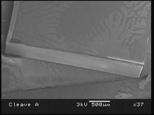
Close up of laser cleaving

Pricing

Contact [email protected] for a quote.

Access and Support

For engineering support questions and to request access, contact [email protected].

Overview

  • The estimated turnaround time for this service is four to six weeks.
  • Processing takes place at INO.
  • Laser is used to trigger the location of cleaving.
  • The cleaving is done with an accuracy of +/-15 µm.
  • The technique provides good facet quality for end-fire coupling.
  • Thin Silicon layers are accepted (up to 5 µm).
  • For chip dimensions, see Guidelines for Laser Assisted Cleaving.
  • We recommend alignment marks on chips to indicate where the cleaving is needed.

Applications

  • Intended for use with Silicon photonics and other Silicon-based chips
  • Cleaving along vertical plane of the waveguide
  • Singulation of specific area of a chip
Scroll to Top
Our office is closed today in observance of Canada Day and will resume operations on the next business day. We’ll respond to your message as soon as possible when we’re back.
Wishing you a wonderful and safe Canada Day!
Skip to content