
TSMC

tsmc logo

TSMC 0.35 µm CMOS Process Technology

This 0.35 μm CMOS technology is available through CMC’s multi-project wafer service, which delivers Taiwan Semiconductor Manufacturing Company (TSMC) nanometer and micron-scale CMOS technologies. Applications The 0.35 µm CMOS (CMC term is CMOSP35) process is suitable for: Analog circuits RF circuits Mixed-signal circuits Process Details Electrical Contact Forming Technology: Polycide Layers: 4 metal, 2 poly Supply Voltages:

TSMC 0.35 µm CMOS Process Technology Read More »

tsmc logo

TSMC 0.13 µm CMOS RF Mixed-Signal Process

CMC’s multi-project wafer service is offering the TSMC(CR013G) RF Mixed-Signal technology. This technology has potential applications in RF and mixed-signal systems, and is suitable for: RF and Mixed-signal designs High-speed digital circuits The CR013G PDK is available on CMC’s STC. If you do not have STC access, or require TSMC libraries, please contact [email protected]. For more

TSMC 0.13 µm CMOS RF Mixed-Signal Process Read More »

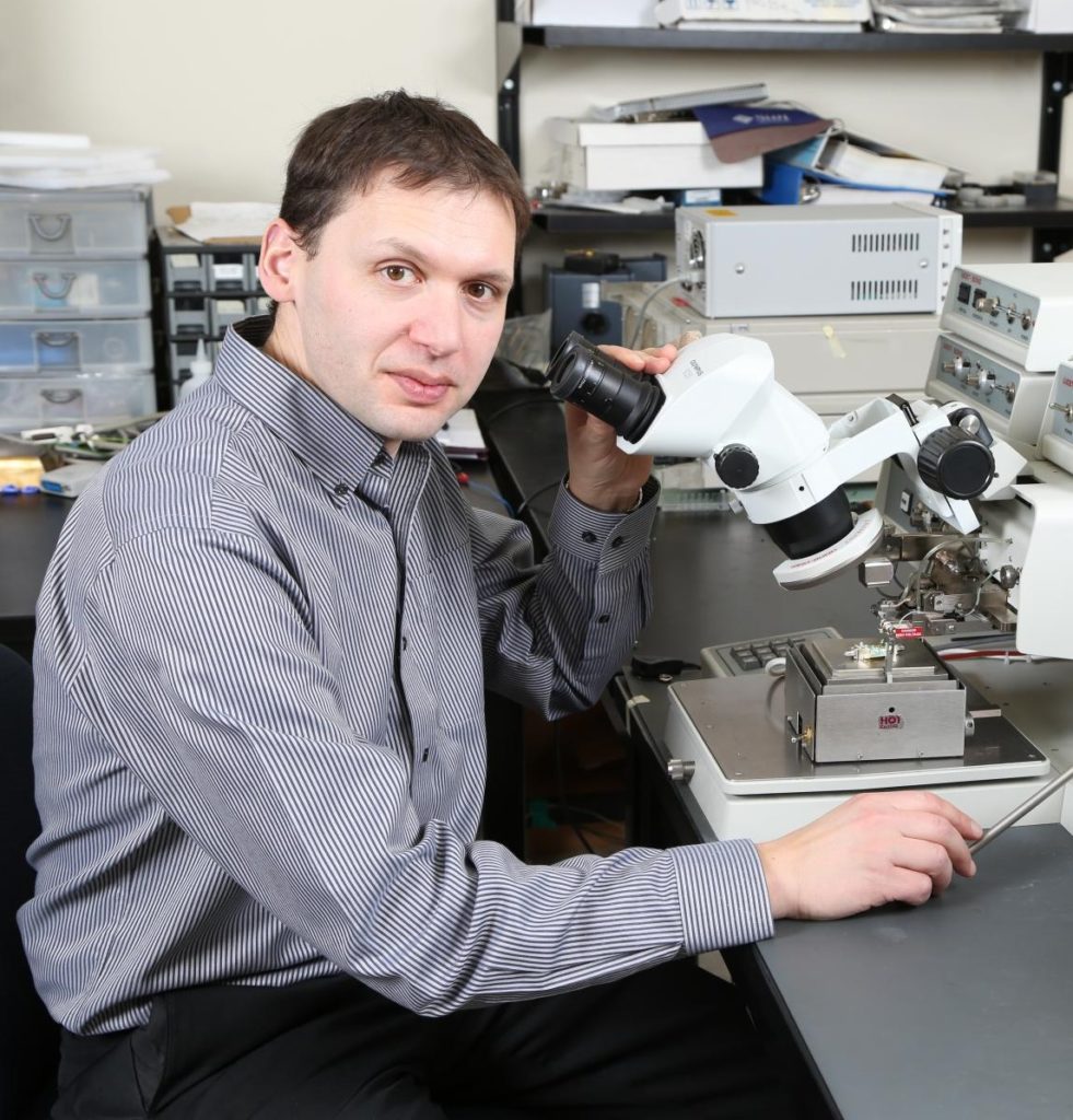
Photo of Dr. Leonid Belostotski working in a lab

Novel receivers target world’s largest radio telescope

Dr. Leonid Belostotski’s pioneering development of focal plane arrays with low-noise receivers is solving a
major problem in cosmic research while creating novel technologies with broad commercial potential. The
University of Calgary researcher’s work is part of a global effort to build the world’s largest radio telescope
for transformational research into the evolution of our universe.

Novel receivers target world’s largest radio telescope Read More »

Scroll to Top
Our office is closed today in observance of Canada Day and will resume operations on the next business day. We’ll respond to your message as soon as possible when we’re back.
Wishing you a wonderful and safe Canada Day!
Skip to content