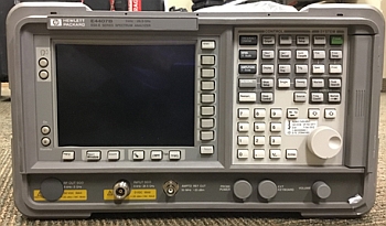
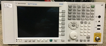
Photo of National Instruments RF PXIe System Including a 26-GHz VSA

National Instruments RF PXIe System Including a 26-GHz VSA

The NI RF PXI-express system, available from the CMC Equipment Rental Program, is an 18-slot PXI-express chassis with high-speed controller (Intel quad core, 4 G memory and Dual OS), 6.6 GHz RF Vector Signal Generator, 26GHz GHz RF Vector Signal Analyzer, Source Measurement Unit, 1.5GHz Oscilloscope, 6.6GHz Vector Signal Generator. This system is an integrated, modular instrument with LabVIEW-based simulation/test environment which enables faster RF test and validation setup and experimental results.

National Instruments RF PXIe System Including a 26-GHz VSA Read More »

Photo of National Instruments PXI System with Two FPGAs, Image Acquisition Module, Digital Multimeter, and an Arbitrary Waveform Generator

National Instruments PXI System with Two FPGAs, Image Acquisition Module, Digital Multimeter, and an Arbitrary Waveform Generator

Modular hardware, managed with LabVIEW software, can be customized for a variety of applications including MEMS and microfluidics testing, video acquisition and processing, particle tracking, pattern matching and general-purpose data acquisition.

National Instruments PXI System with Two FPGAs, Image Acquisition Module, Digital Multimeter, and an Arbitrary Waveform Generator Read More »

Photo of National Instruments PXI System with an FPGA, Arbitrary Waveform Generator, Scope, and Digital Multimeter

National Instruments PXI System with an FPGA, Arbitrary Waveform Generator, Scope, and Digital Multimeter

Modular hardware, managed with LabVIEW software, can be customized for a variety of applications including MEMS and microfluidics testing, video acquisition and processing, particle tracking, pattern matching and general-purpose data acquisition.

National Instruments PXI System with an FPGA, Arbitrary Waveform Generator, Scope, and Digital Multimeter Read More »

Photo of 8970B

Agilent (Hewlett-Packard) 8970B Noise Figure Meter

The Agilent 8970B makes noise figure measurements in the 0 to 30 dB range. Measured noise can be displayed as noise figure or equivalent input noise temperature. Excess Noise Ratio (ENR) data can be entered in data tables on the noise figure meter. The meter uses this information to correct for ENR vs. frequency variations. The 8970B can be used with Agilent 346 (CMC loans the Agilent 346B Solid State Noise Source separately) or 347 noise sources.

Agilent (Hewlett-Packard) 8970B Noise Figure Meter Read More »

Photo of Agilent 87405A

Agilent 87405A Preamplifier, 10 MHz to 3 GHz

The 87405A Preamplifier is a multi-purpose instrument for any application that requires low noise and additional gain. The SNR of the final signal in an RF system is greatly impacted by the initial amplification of the signal and its original SNR. By having low noise figure in a preamplifier, the final signal will have a lower noise than without the preamplifier.

Agilent 87405A Preamplifier, 10 MHz to 3 GHz Read More »

Keysight RF PXIe System (upgraded M9381A)

This Keysight RF PXI-express system chassis, is an 18-slot chassis with a high-speed controller (Intel i7 with 16GB RAM) and a variety of RF and FPGA cards. The system includes a Vector Signal Analyzer (6.6GHz), a Vector Signal Generator (6 GHz with a reference frequency generator), DC power supply, digital I/O’s, Kintex-7 FPGA board, and several supporting accessories for a complete benchtop RF test environment.

Keysight RF PXIe System (upgraded M9381A) Read More »

Photo of Keysight_M9375A

Keysight 6-port VNA (M9375A)

The Keysight Vector Network Analyzer (VNA) comes with a wide bandwidth for 5G research and offers full 6-port analysis. It can also be combined with multiple Keysight VNAs for MIMO research and includes an automated electronic calibration kit to simplify and speed the process of getting the correct measurements quickly. Also available from CMC, these VNAs can be used with a Keysight Materials measurement suite software (N5100A) and dielectric probe kit to allow for research in dielectric resonators and interfacing with biological systems. The VNA is housed in an 18-slot M9019A Gen 3 Chassis and uses an M9037A Controller with a swappable SSD drive.

Keysight 6-port VNA (M9375A) Read More »

CADpass

  for    Download CADpass Client Getting Started Quick Start Guide: CADpass Client for Windows Quick Start Guide: CADpass for Linux Quick Start Guide: CADpass for MAC Resources Licensing Information CAD Tool Quick Start Guides FAQ for CADpass

CADpass Read More »

How can I acknowledge the ways CMC has advanced my research?

If your research benefits from products and services provided by CMC Microsystems, please acknowledge this support in any publications about your work. Thank you for your support. Acknowledgment Text Examples We would like to acknowledge CMC Microsystems, manager of the FABrIC project funded by the Government of Canada, for the provision of products and services that

How can I acknowledge the ways CMC has advanced my research? Read More »

Financial Assistance Payments

The MicroFAB Access supports custom microfabrication projects at open-access facilities MicroFAB Access reimbursement: 80% of the eligible fabrication costs. The Student’s academic supervisor must hold a CMC Subscription. The reimbursement is payable by EFT/ to the institution.Email: finance@cmc.ca If you have any questions please contact us: MicroFAB Access Team

Financial Assistance Payments Read More »

MEMSCAP 'The Power of a Small World' logo

Science Foundry Post-Processing for Poly MEMS

In partnership with Science Foundry, CMC offers users access to the Poly MEMS technology. Poly MEMS technology is a triple polysilicon, single metal surface micromachining process with deposited oxide (PSG) as the sacrificial material, and silicon nitride for electrical isolation from the substrate. Post-processing for Poly MEMS offers optional HF release and supercritical carbon dioxide

Science Foundry Post-Processing for Poly MEMS Read More »

MEMSCAP 'The Power of a Small World' logo

Science Foundry Poly MEMS Multi-User MEMS Process Technology

CMC’s multi-project wafer service delivers the MEMS technology, through a partnership with Science Foundry. The Poly MEMS technology is a triple polysilicon, single metal surface micromachining process with deposited oxide (PSG) as the sacrificial material, and silicon nitride for electrical isolation from the substrate. CMC also offers optional HF release and supercritical carbon dioxide drying.

Science Foundry Poly MEMS Multi-User MEMS Process Technology Read More »

Teledyne Micralyne logo

Teledyne Micralyne Micralyne MicraGEM-Si™ MEMS Process

Micralyne MicraGEM-SiTM is a silicon-on-insulator (SOI) based MEMS process which will reduce the initial cost and risk of prototype development, while speeding the time to market for MEMS- Based devices. MicraGEM-SiTM is ideally suited for the manufacture of tilting mirrors and mirror arrays for variable optical attenuators (VOA) and wavelength selective switch (WSS) modules, commonly used in

Teledyne Micralyne Micralyne MicraGEM-Si™ MEMS Process Read More »

AMF Silicon Photonics General-Purpose Fabrication Process

Silicon-on-insulator, 220-nm top Si film, 3000-nm buried oxide (BOX) High resistivity handle wafer (>750 ohm-cm) 193-nm deep UV lithography for waveguides, enabling features down to approximately 140 nm Two partial etches and one full etch of the top silicon PECVD Silicon Nitride waveguide integration 6 implants for optical modulators (P++, P+, P, N++, N+, N) Germanium

AMF Silicon Photonics General-Purpose Fabrication Process Read More »

AMS 0.35 µm CMOS Process Technology (High-Voltage)

This 0.35 µm CMOS technology offers four metal layers, digital standard cells, an anti-reflective coating and high-efficiency photodiodes, and bulk micromachining. CMC’s multi-project wafer service delivers this technology from austriamicrosystems, offering three processes: Basic, Opto and High-Voltage (see details below). The technology is suitable for: High-Voltage Process (H35B4D3) Details Technology Features: 4 metal and 2 poly layers with a

AMS 0.35 µm CMOS Process Technology (High-Voltage) Read More »

AMS 0.35 µm CMOS Process Technology (Opto)

This 0.35 μm CMOS technology offers four metal layers, digital standard cells, an anti-reflective coating and high-efficiency photodiodes, and bulk micromachining. CMC’s multi-project wafer service delivers this technology from austriamicrosystems, offering three processes: Basic, Opto (see details below) and High-Voltage. Opto Process (C35B4O1) Details Technology Features: 4 metal and 2 poly layers (similar to basic option) High-efficiency

AMS 0.35 µm CMOS Process Technology (Opto) Read More »

AMS 0.35 µm CMOS Process Technology (Basic)

This 0.35 μm CMOS technology offers four metal layers, digital standard cells, an anti-reflective coating and high-efficiency photodiodes, and bulk micromachining. CMC’s multi-project wafer service delivers this technology from austriamicrosystems, offering three processes: Basic (see details below), Opto and High-Voltage. Basic Process (C35B4C3) Details Technology Features: 4 metal and 2 poly layers Supply Voltage: 3.3/5V Bulk-micromachining option, allowing

AMS 0.35 µm CMOS Process Technology (Basic) Read More »

tsmc logo

TSMC 0.35 µm CMOS Process Technology

This 0.35 μm CMOS technology is available through CMC’s multi-project wafer service, which delivers Taiwan Semiconductor Manufacturing Company (TSMC) nanometer and micron-scale CMOS technologies. Applications The 0.35 µm CMOS (CMC term is CMOSP35) process is suitable for: Analog circuits RF circuits Mixed-signal circuits Process Details Electrical Contact Forming Technology: Polycide Layers: 4 metal, 2 poly Supply Voltages:

TSMC 0.35 µm CMOS Process Technology Read More »

STMicroelectronics - Life Augmented

STM 28nm FD SOI CMOS

The latest product information can be found at: http://mycmp.fr/datasheet/ic-28nm-cmos28fdsoi. To start the 28-nm licensing process, please submit your design kit request to CMP directly through the link: https://mycmp.fr/requests/design-kit-141.html. Notes: STMicroelectronics prohibits use of this 28-nm technology for any medical or military applications. The expected number of chips to be delivered for this technology is 30.

STM 28nm FD SOI CMOS Read More »

Synopsys Design Tools

Synopsys provides a comprehensive portfolio of tools for silicon design, synthesis and verification. Software tools available in this bundle include: Custom Design Digital Design Silicon Lifecycle Management Verification For more information, see the Synopsys University Program. For more information about the software available for the current year, refer to the Support Note: Synopsys 2025 Annual Bundle

Synopsys Design Tools Read More »

SolidWorks logo

SolidWorks Software Packages

SolidWorks Software Packages cover 2D and 3D part modelling, large assembly design, sheet metal and weldments, surfacing, molds, product configuration, and 3D rendering and design analysis for manufacturing and computer-aided manufacturing (CAM). For a full list of the SolidWorks tools available in this package, please refer to the SolidWorks Quick Start Guide. We offer Standard and

SolidWorks Software Packages Read More »

Optiwave OptiSuite

The OptiSuite toolset includes: OptiSystem – a comprehensive software design suite that enables users to plan, test, and simulate optical links in the transmission layer of modern optical networks. OptiInstrument – addresses the needs for working with instruments. OptiSPICE – is used to analyze integrated circuits, including interactions of optical and electronic components. It allows

Optiwave OptiSuite Read More »

National Instruments logo

National Instruments LabView Design Tool

The NI LabVIEW is a software tool for creating and deploying measurement and control systems. It supplies an integrated environment for design, simulation, instrument control, hardware-in-the-loop verification, and microsystem device characterization and validation. LabVIEW is also a central tool in the current Microsystem Integration Platform configuration. The software drivers included with LabVIEW and many other

National Instruments LabView Design Tool Read More »

Siemens logo

Siemens Higher Education Program

The Canadian Academic Siemens Higher Education Program offering for National Design Network researchers includes: IC Nanometer Design—Tanner S-Edit, L-Edit, T-Spice, Eldo ®, Questa ® ADMS, Nitro-SoCTM, Oasys-RTL, Calibre®, IE3D Design, Verification and Test—Catapult ® Ultra, VistaTM, ReqTracerTM, Questa (including ModelSim®), Oasys-RTL, Precision ® Synthesis, LeonardoSpectrumTM ASIC, Tessent ® Silicon Test, SystemVision® PCB PADS/Hyperlynx—PADS Standard Plus with HyperLynx

Siemens Higher Education Program Read More »

Luceda IPKISS Photonics Design Tool

Luceda IPKISS is a Silicon Photonics design tool. It can be used with Tanner design suite to form an integrated design environment, with the following features: IPKISS’ PICAZZO library Python-based Pcells Silicon Photonics Schematic design capability through Tanner S-Edit Circuit simulation with CAPHE simulator Silicon Photonics Schematic-driven layout (SDL) generation Layout design and manual modification

Luceda IPKISS Photonics Design Tool Read More »

Keysight Technologies PathWave Software Platform

Keysight Technologies PathWave software platform is a set of CAD tools for high-frequency system, circuit and modelling applications. The following products are available to subscribers: Advanced Design System (ADS) — Circuit design and simulation software with extensive libraries and design guides; EM Design (EMPro) — Electromagnetic modelling and simulation software for 3D components; RF Synthesis (Genesys) —RF

Keysight Technologies PathWave Software Platform Read More »

intel FPGA logo

Altera Development Tools

The Intel FPGA Development tools include the following software: Quartus Prime (both Standard and Pro. Edition)—provides a complete, multi-platform design environment for Intel FPGA, SoCs, and CPLDs. It includes tools to enable users to perform from design entry and synthesis to optimization, verification, and simulation, including partial reconfiguration for the supported device families such as

Altera Development Tools Read More »

Thermo Fisher Scientific Amira-Avizo Visualisation and Analysis Software

Amira and Avizo are data visualisation, analysis and modeling software programs. These suites allow you to explore and analyze data sets from widely different disciplines, including: Physics, Geology: Electrostatic fields; Magnetic fields; Tensor fields; Core sample study Chemistry, Life Sciences: Molecular surfaces and interfaces, dynamics; Granulometry Material Science: Non-destructive testing; Tomographic imaging and microscopy Mechanical

Thermo Fisher Scientific Amira-Avizo Visualisation and Analysis Software Read More »

Design Workshop dw-2000 Photonic Design Software

The dw-2000™ Physical Layout and Verification Software, from Design Workshop Technologies Inc., enables the physical layout and verification of optical components built using planar waveguide technology and other semiconductor manufacturing techniques, such as microwave designs. dw-2000 has many benefits for photonic layout applications while avoiding the pitfalls associated with the use of a general-purpose drawing tool.

Design Workshop dw-2000 Photonic Design Software Read More »

Computer server storage units and cloud in background. 3d illustration

CMC Cloud Design Environment

CMC Cloud provides secure, high-performance, remotely accessible EDA resources for the design of advanced microsystems and nanotechnologies. Quick Start Guides Access CMC Cloud Turbo Access CMC Cloud VCAD Access with a Research Subscription What You Get Secure Design Environment: When using CMC Cloud, you have a robust and supported design environment that is securely delivered

CMC Cloud Design Environment Read More »

CoventorMP MEMS Design Platform

CoventorMP (MEMS+ and CoventorWare) provides 3D MEMS simulation, analysis, and design automation software for the development of micro- and nano-scale devices and systems. These modules cover the full MEMS design flow for system-level simulation, layout generation, and finite element analysis (FEA) and model generators for IC simulators. The list includes: CoventorWare Designer for MEMS physical design,

CoventorMP MEMS Design Platform Read More »

COMSOL logo

COMSOL Multiphysics

The COMSOL Multiphysics engineering simulation software environment facilitates all steps in the modelling process − defining your geometry, meshing, specifying your physics, solving, and then visualizing your results. COMSOL provides software solutions for multiphysics modelling. Through CMC, you can access the following: Finite element analysis (FEA) and simulation capabilities Modelling capabilities for defining geometry, meshing and physical

COMSOL Multiphysics Read More »

Scroll to Top
Skip to content